
Split-block waveguide alignment is controlled by the complete locating interface, not by dowel pins alone. The two halves must register the machined waveguide features to one another while the mating faces close consistently under the specified fastener pattern. Pin position and fit, face flatness and cleanliness, screw clearance, groove-to-datum location, and assembly sequence can all contribute to the final offset. The right drawing strategy is to define which half owns the reference geometry, how the second half is located, and what assembled feature or RF result is being accepted. Pin count or nominal pin diameter by itself does not prove alignment; those details must be related to the interface and verified at the assembly condition.
Define the interface before choosing pins
A split-block design divides a waveguide channel between mating components. The assembled channel depends on the geometry in each half and on how the halves return to the same relative position after separation. Alignment pins can improve repeatability, but they work only when their locations and fits are referenced to the waveguide features and the mating faces.
Begin with the part’s functional interface: waveguide port, flange or transition features, channel centerline, sealing or contact land, and fastener locations. Decide whether the channel is centered from one half or dimensioned symmetrically across the joint. Avoid dimensioning each half independently from unrelated edges, because the resulting tolerance stack can shift the assembled channel even when each component meets its own local dimensions.
Mechanical alignment and RF performance are linked but not interchangeable. The project’s frequency range, mode, transition geometry and test method determine which offsets or discontinuities matter. Those requirements belong to the responsible RF design and acceptance plan, not to an assumed universal machining tolerance.
Control the datum chain across both halves
Choose a primary datum on the interface that can be inspected and reproduced, often a mating face or a defined assembly plane. Locate the critical channel features and pin holes from that datum system. The opposing half should use a coordinated datum scheme so that channel centerlines, steps and ports meet when assembled, not merely when each block is measured on its own setup.
Datum transfer deserves explicit attention. If one half is machined from a port datum and the other from an outside wall, their individual coordinate systems can disagree. A common datum strategy, matched machining approach, or controlled assembly inspection can reduce ambiguity. The selected method depends on the design and available inspection access.
Allow for the tolerance stack from pin location, hole location, fit clearance, face seating and fastener movement. A close pin fit may improve location but can also make assembly sensitive to burrs, thermal changes or small positional errors. More pins are not automatically better if the pattern over-constrains the interface.
Design pins, holes, screws, and faces as one system
Alignment pins establish in-plane location; the mating faces establish seating and orientation; screws provide clamping force. Drawings should make those roles clear. Use controlled pin-hole relationships and identify whether the pins are fixed in one block, removable, or part of a separate assembly element. Fastener holes should not accidentally become competing locating features unless the design intentionally uses them that way.
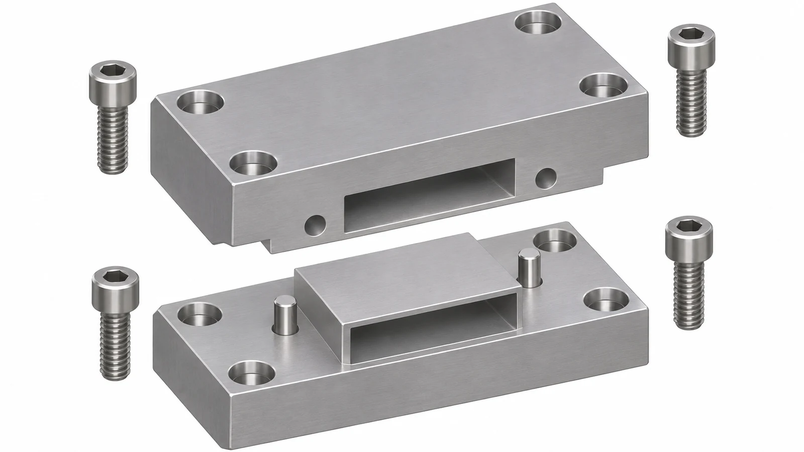
| Caractéristique | Alignment role | Question de revue |
|---|---|---|
| Mating face | Seats the two halves and controls interface plane | Are flatness, finish, cleanliness and contact regions defined? |
| Pin and hole pattern | Re-establishes relative in-plane position | Are fits, location datums and assembly direction specified? |
| Fixations | Clamps the joint | Can clearance or tightening sequence shift the halves? |
| Waveguide channel | Defines the functional passage | Are both halves located from a coordinated datum system? |
La précision Fraisage CNC and multi-axis access can be relevant to the geometry, but the actual feature strategy depends on the released design. When several faces or ports must relate, review the datum sequence and inspection method before releasing the split line.
Inspect the assembled geometry that matters
Component inspection should verify the mating faces, pin locations, channel features and datum relationships individually. Assembly inspection then checks whether the halves close and locate as intended. Depending on the design, this may include a step or offset across the split, port registration, a gauge feature, coordinate measurement, or another method agreed in the acceptance plan.
Measure at the same clamping condition that represents service or test. Loose parts sitting together by gravity may not reproduce the position after fasteners are tightened. Conversely, an inspection fixture that forces the blocks into alignment can hide a mismatch. Document the fixture, torque or tightening sequence when those conditions affect the result.
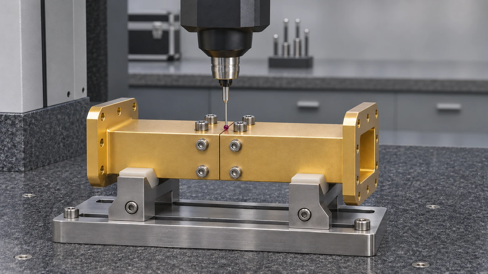
Keep mechanical inspection distinct from RF testing. If electrical/RF performance is the final acceptance criterion, define the test setup, calibration and test limits separately. A mechanically acceptable alignment result can support the RF evaluation but does not establish the complete device performance by itself.
Connect mechanical alignment to RF acceptance
Research examples of CNC-machined waveguide assemblies use pins or dowels to align split blocks, but their geometries, frequencies and test conditions are specific to those designs. The lesson is to control repeatable assembly and verify the functional device, not to copy a pin size, count or positional tolerance from a different waveguide.
Before release, have mechanical and RF owners agree on the interface datums, permitted channel discontinuities, pin strategy, assembly condition and evidence required. Include both component-level dimensions and any assembled checks in the drawing package. The resulting plan can then be inspected without guessing whether the decisive requirement is a pin fit, a channel step, a port offset, or a measured RF response.