
Introducción: El papel crítico de la carcasa del módulo óptico en las redes modernas
En las arterias invisibles de nuestro mundo digital—las vastas redes de fibra óptica que transportan nuestros datos, transmisiones de video y servicios en la nube—innumerables componentes deben funcionar en perfecta armonía. En el corazón de esta conectividad, conectándose a routers, switches y servidores, se encuentran los módulos transceptores ópticos. Estos módulos son los traductores esenciales, que convierten señales eléctricas en luz y viceversa. Pero esta sofisticada tecnología interna sería frágil, poco confiable e incompatible sin su primera línea de defensa y su interfaz principal: la carcasa del módulo óptico. Esta cubierta exterior es mucho más que una simple tapa; es un componente de ingeniería crítico que define la identidad física del módulo, garantiza su estabilidad térmica y eléctrica, y asegura que pueda insertarse sin problemas en equipos de cualquier fabricante importante a nivel mundial. La búsqueda incesante de mayores velocidades de datos, de 100G a 800G y más allá, impone demandas sin precedentes a estas carcasas. Su papel en el mantenimiento de la integridad de la señal, la gestión de intensas cargas de calor y la habilitación del empaquetado denso de puertos en los centros de datos modernos es absolutamente fundamental para el rendimiento y la disponibilidad de la red. Comprender la carcasa del módulo óptico es, por lo tanto, clave para entender la capa física de nuestra infraestructura conectada.
¿Qué es una carcasa de módulo óptico? Definiendo la base
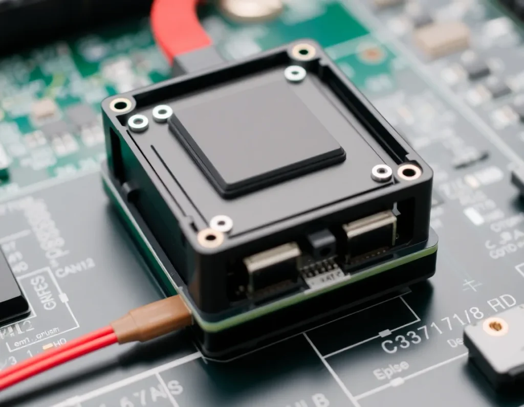
Una carcasa de módulo óptico es el recinto estandarizado de metal o de metal y plástico que contiene y protege los componentes principales de un transceptor óptico. Piense en ella como el chasis o esqueleto del módulo. En su interior, elementos delicados como el transmisor láser, el receptor de fotodiodo, los CI controladores y la circuitería de control están montados en una placa de circuito impreso (PCB). La carcasa proporciona la estructura rígida que mantiene estos componentes en una alineación precisa, en particular para los subconjuntos ópticos que deben interconectarse perfectamente con el conector de fibra óptica. De manera crucial, la carcasa no es un diseño personalizado para cada módulo; se adhiere a estrictos acuerdos de múltiples fuentes (MSA) que definen cada una de sus dimensiones externas, el mecanismo de bloqueo del conector y la disposición de los pines eléctricos. Esta estandarización es lo que permite a un ingeniero de redes comprar un módulo QSFP28 de un fabricante y conectarlo con confianza a un switch de otro, sabiendo que encajará y funcionará. La carcasa también integra el puerto de fibra LC dúplex o MPO en la parte frontal y el conector eléctrico de borde (los “dedos dorados”) en la parte posterior. En esencia, la carcasa es el puente físico y mecánico entre el frágil mundo de la optoelectrónica y el robusto y estandarizado mundo del hardware de red.
Funciones principales y principios de diseño de las carcasas de módulos ópticos
El diseño de una carcasa de módulo óptico es un complejo acto de equilibrio impulsado por varias funciones no negociables. Cada principio impacta directamente en la fiabilidad y la interoperabilidad del módulo.
Interfaz mecánica e interoperabilidad
La función principal es proporcionar una interfaz mecánica impecable con la jaula y el conector del dispositivo anfitrión. Las dimensiones de la carcasa, la ubicación y el diseño de su pestillo, y la colocación de sus orificios de montaje deben ser exactos. Incluso una desviación mínima puede impedir la inserción, causar un contacto eléctrico deficiente o dañar los sensibles pines del conector del anfitrión. El diseño prioriza una sensación de inserción y extracción suave y positiva, a la vez que garantiza una conexión segura y resistente a las vibraciones.
Protección de componentes e integridad estructural
La carcasa actúa como un escudo robusto contra daños físicos, polvo y contaminantes. Protege la PCB interna y los componentes de las tensiones cotidianas de manipulación, impactos accidentales y las fuerzas mecánicas involucradas en el acoplamiento y desacoplamiento de los cables de fibra. La estructura debe ser lo suficientemente rígida como para evitar la flexión, que podría desalinear los componentes ópticos o agrietar las uniones soldadas, pero a la vez diseñada para un ensamblaje eficiente durante la fabricación.
Ruta de conducción térmica
Quizás uno de sus roles más críticos es servir como el principal disipador de calor. Los láseres y procesadores de alta potencia generan una cantidad significativa de calor. La carcasa está diseñada para extraer este calor de los componentes internos, normalmente mediante contacto directo con la PCB y los chips clave, y transferirlo a la jaula metálica más grande del sistema anfitrión, que cuenta con su propia solución de refrigeración. Toda la superficie inferior de la carcasa suele actuar como placa de transferencia térmica.
Contención de interferencias electromagnéticas (EMI)
Las señales eléctricas de alta velocidad dentro de un módulo pueden irradiar ruido electromagnético, que puede interferir con la electrónica cercana. A la inversa, el módulo necesita protección contra EMI externas. El cuerpo metálico de la carcasa forma una jaula de Faraday, que contiene las emisiones internas y protege los circuitos sensibles de interferencias externas. Las aberturas y las juntas están meticulosamente diseñadas para minimizar las fugas de RF.
Materiales clave y procesos de fabricación para la durabilidad y el rendimiento
La elección de los materiales y la forma en que se conforman es fundamental para lograr los principios de diseño descritos anteriormente. El rendimiento, el costo y la fabricabilidad son consideraciones clave.
Materiales principales
- Metales (para el cuerpo principal): La aleación de zinc fundida a presión es el material tradicional y más común. Ofrece un excelente apantallamiento EMI, buena conductividad térmica y alta resistencia para formas intrincadas a un costo relativamente bajo. Para módulos de mayor rendimiento, especialmente aquellos que generan más calor, a veces se utilizan aleaciones de cobre o aluminio por su superior conductividad térmica, aunque pueden ser más costosos y más difíciles de fundir a presión con detalles finos. El acero inoxidable se utiliza a menudo para el resorte del pestillo y otras piezas mecánicas críticas por su durabilidad y propiedades elásticas.
- Plásticos (para biseles y componentes): Se utilizan plásticos de ingeniería de alta temperatura y alta resistencia como LCP (polímero de cristal líquido) o PPS (sulfuro de polifenileno) para el bisel frontal que aloja los puertos de fibra. Estos materiales pueden soportar el calor de la soldadura durante el ensamblaje, proporcionar aislamiento eléctrico y ofrecer un moldeo preciso para las delicadas interfaces de adaptadores de fibra.
Procesos de fabricación
- Fundición a presión: Este es el proceso estándar para las carcasas metálicas. El zinc o el aluminio fundidos se inyectan a alta presión en un molde de acero de precisión (dado). Esto permite la producción en masa de piezas complejas de forma neta con buena precisión dimensional, esencial para la interoperabilidad. Después de la fundición, las piezas se recortan, se desbarban y, a menudo, se recubren (por ejemplo, con níquel) para resistir la corrosión y mejorar el contacto superficial para el rendimiento EMI y térmico.
- Mecanizado de precisión: Se utiliza para series de prototipos, producción de muy bajo volumen o para crear características específicas de alta tolerancia en una pieza fundida a presión. Es más costoso y más lento que la fundición a presión.
- Injection Molding: Used for the plastic bezel and internal components. This process allows for high-volume, cost-effective production of parts with excellent detail, such as the snap-fits and guides for the fiber connector.
- Assembly and Welding: The final housing is often an assembly of several pieces. The metal top and bottom halves are typically laser-welded or fixed with screws. Laser welding creates a hermetic, continuous seam that maximizes EMI shielding and structural integrity without introducing additional materials like adhesives that could outgas or degrade.
Types and Form Factors: From SFP to QSFP-DD and Beyond
The evolution of data rates and port density has driven the development of a family of standardized form factors, each with its own distinct housing design. The form factor name essentially defines the housing’s size, shape, and electrical interface.
- SFP (Small Form-factor Pluggable): The workhorse of the industry for 1G/10G applications. Its compact, narrow housing is designed for high port density. Variations include SFP+ (enhanced for 10G/16G/25G) and SFP28 (for 25G). The housing is relatively simple but must still manage heat and EMI effectively.
- SFP-DD (Double Density): An evolution of SFP that doubles the port density by using two electrical lanes in the same width as a standard SFP. The housing is slightly deeper to accommodate the more complex internal layout and additional electrical contacts.
- QSFP (Quad Small Form-factor Pluggable): Significantly wider than SFP, designed to carry four lanes of data. This housing must manage substantially more heat and more complex internal routing. Its variants define generations: QSFP+ (40G), QSFP28 (100G), and QSFP56 (200G).
- QSFP-DD (Double Density): The leading high-density form factor for 400G and 800G. It builds on the QSFP width but adds a second row of electrical contacts (making it “double density”) to support eight high-speed electrical lanes. The housing design is a marvel of miniaturization and thermal engineering, as it packs immense processing power into a space not much larger than a QSFP28.
- OSFP (Octal Small Form-factor Pluggable): A slightly wider and deeper alternative to QSFP-DD for 800G applications. Its housing is designed from the outset for higher power dissipation, often incorporating a more robust thermal solution, such as an integrated heat sink for direct airflow.
- CFP (C Form-factor Pluggable): A much larger form factor used for early 100G and now for very high-power, long-reach applications like 400ZR coherent optics. Its large housing is necessary to accommodate complex electronics, larger lasers, and more sophisticated cooling solutions.
Each step in this progression represents a housing engineering challenge: packing more functionality into a constrained space while managing increased power and heat.
Thermal Management: How Housings Dissipate Heat for Reliability
As data rates skyrocket, the power consumption of optical modules has followed suit. A modern 800G module can easily dissipate 12-15 watts or more. If this heat is not effectively removed, component temperatures soar, leading to accelerated aging, increased bit error rates, wavelength drift in lasers, and ultimately, catastrophic failure. The carcasa del módulo óptico is the central player in the thermal management system.
The thermal path begins inside the module. The hottest components, like the laser driver and DSP chip, are designed to transfer heat into the module’s PCB through thermal vias and pads. The PCB itself then conducts this heat to the metal baseplate of the housing, which is in direct mechanical contact with it. This baseplate is the workhorse of the thermal system. It spreads the heat across its entire surface area.
The next critical interface is between the housing’s baseplate and the host system’s cage. When the module is fully inserted, this metal-to-metal contact is the primary conduit for transferring heat out of the module. To optimize this, the housing baseplate is often machined flat and may even be lightly coated with a thermal interface material (TIM) like grease or a phase-change pad to fill microscopic air gaps that act as insulators.
The host cage is typically attached to a large thermal mass or heat sink on the system board, and often sits in the path of forced airflow from system fans. In some advanced designs, like the OSFP form factor, the housing itself may extend upward to present fins or a raised surface directly into the airflow, acting as an integrated heat sink. For the highest-power coherent modules, the housing may even be designed to interface with a cold plate for liquid cooling. Every aspect of the housing’s material, geometry, and surface finish is scrutinized for its impact on thermal impedance, making it a defining factor in the module’s performance envelope and reliability.
Mechanical and EMI Shielding: Protecting Sensitive Internal Components
Beyond managing heat, the carcasa del módulo óptico serves as the first and most critical line of defense against physical and electromagnetic threats. The sensitive integrated circuits, lasers, and photodiodes inside a module are fragile and operate at high frequencies, making them vulnerable to damage from shock, vibration, and external interference. The housing’s mechanical integrity is therefore paramount. It is engineered to withstand the rigors of insertion and extraction, often thousands of cycles over its lifetime, without deforming. The latching mechanism, typically a bail or button-style design, is integrated into the housing and must provide secure retention in the host cage while allowing for smooth, tool-less removal. The housing also protects against dust and other contaminants, with tight tolerances and sometimes gasketing to prevent particulate ingress that could cloud optical interfaces or cause electrical shorts.
Perhaps an even more sophisticated role is electromagnetic interference (EMI) shielding. High-speed electrical signals inside the module can radiate energy, potentially disrupting nearby electronics. Conversely, external EMI from other system components can couple into the module and corrupt its high-speed data streams. The housing acts as a Faraday cage, enclosing the internal components in a continuous conductive shell. This is why materials like zinc die-cast alloy or steel with conductive plating are favored—they are not just structurally sound but also excellent conductors. The design ensures that when the module is fully inserted, the housing makes a 360-degree electrical contact with the metal host cage, creating an unbroken shielded enclosure. Critical openings, such as the port for the optical connector, are designed with careful attention to the gap size relative to the wavelength of the interference to prevent leakage. This comprehensive shielding is non-negotiable for meeting stringent regulatory emissions standards and ensuring the module functions reliably in the dense, noisy environment of a network switch or router.
Standards and Compliance: Ensuring Interoperability in Global Networks
The true power of optical modules lies in their universality. A module from one manufacturer must seamlessly plug and play in equipment from another, anywhere in the world. This interoperability is not accidental; it is enforced by a complex ecosystem of international standards that dictate nearly every aspect of the carcasa del módulo óptico. Form factor definitions, managed by multi-source agreements (MSAs), are the most visible of these standards. Groups like the Small Form Factor Committee (SFF Committee) and ad-hoc MSA groups for QSFP, OSFP, and others publish detailed mechanical specifications. These documents precisely define the housing’s external dimensions, the position and shape of the latch, the connector port location, and even the labeling area. A deviation of a fraction of a millimeter could prevent a module from fitting into a host cage, so manufacturers adhere to these blueprints with extreme precision.
Compliance extends far beyond physical shape. The housing is central to meeting safety and environmental regulations. For instance, the housing material must often meet flammability ratings like UL 94 V-0. It must also ensure user safety by preventing accidental exposure to laser light, which is managed through the design of the port shutters and internal baffles. Electromagnetic compatibility (EMC) standards, such as those from the FCC (U.S.) and CE (EU), mandate the level of EMI shielding the completed module must achieve, directly validating the housing’s design and material conductivity. Furthermore, standards like Telcordia GR-468-CORE or IEC 62005 outline rigorous reliability testing for mechanical robustness, thermal cycling, and corrosion resistance—tests the housing must survive to prove the module’s worth for carrier-grade networks. This global framework of standards, while complex, is what allows data centers and telecom providers to build heterogeneous, scalable, and reliable networks with confidence.
The Future of Optical Module Housings: Trends and Innovations
As network demands push towards higher speeds, greater density, and lower power, the humble module housing is evolving to meet radical new challenges. The trend toward co-packaged optics (CPO) represents a potential paradigm shift. In CPO architectures, the optical engine is moved much closer to or even onto the same package as the switch ASIC, drastically reducing electrical path lengths. This could eventually lead to the disappearance of the traditional, pluggable module as we know it, replaced by onboard optical assemblies with specialized, integrated housings that focus on thermal and optical coupling rather than hot-swappability. However, pluggables will dominate for the foreseeable future, and their housings are adapting. For the next generation of 1.6T and 3.2T modules, power dissipation will exceed 30 watts, pushing air cooling to its limits. Future housings will increasingly be designed with liquid cooling in mind, featuring integrated microchannels or cold-plate interfaces as a standard option.
Material science is also driving innovation. To reduce weight and improve thermal conductivity, advanced composites and metal matrix composites (MMCs), like aluminum with embedded carbon fibers or diamond particles, are being explored. These materials can offer thermal performance superior to traditional aluminum alloys while being lighter. There is also a push for greater sustainability, leading to research into recyclable polymers and greener plating processes. On the design front, intelligent housings with embedded sensors are on the horizon. Tiny sensors for temperature, humidity, and even physical shock could be integrated into the housing structure, providing real-time telemetry for predictive health monitoring of the module and the broader system. Finally, as form factors like QSFP-DD and OSFP reach their electrical I/O limits, new housing designs will emerge to support even higher lane counts and novel internal architectures, all while maintaining backward compatibility or defining new standards for the next era of connectivity.
Resumen de puntos clave
The optical module housing is a deceptively complex component that is fundamental to the function and reliability of modern high-speed networks. It is far more than a simple metal shell. Its primary roles are multifaceted: it provides the critical mechanical structure and latching mechanism for secure, hot-swappable operation; it acts as the essential thermal path, conducting waste heat from internal components to the host system; and it serves as a comprehensive shield, protecting sensitive electronics from physical damage and electromagnetic interference. The choice of materials—typically zinc, aluminum, or advanced composites—is driven by the need for strength, thermal conductivity, and EMI suppression.
The housing’s design is almost entirely dictated by industry standards and multi-source agreements (MSAs), which ensure interoperability across vendors and form factors, from SFP to QSFP-DD and OSFP. Compliance with these mechanical, safety, and EMC standards is non-negotiable for global market acceptance. Looking ahead, the housing will continue to evolve to address the challenges of higher power densities, likely incorporating advanced liquid cooling interfaces, smarter materials, and even integrated sensor technology. As optical technology advances toward co-packaged optics and beyond, the housing’s role may transform, but its core mission of enabling reliable, high-performance connectivity will remain central to the architecture of our digital world.
Preguntas frecuentes (FAQ)
What is the main purpose of an optical module housing?
The housing serves three equally vital purposes. First, it provides the mechanical structure, including the latching mechanism, that allows the module to be securely inserted, retained, and hot-swapped in network equipment. Second, it acts as the primary heat sink, drawing thermal energy away from the high-power lasers and electronics inside and transferring it to the host system. Third, it forms a conductive Faraday cage that shields the module’s internal components from electromagnetic interference (EMI) and prevents the module itself from emitting disruptive signals.
Why are most optical module housings made of metal?
Metal, specifically die-cast zinc or aluminum alloys, is the material of choice because it uniquely combines several necessary properties. It is mechanically strong to withstand insertion cycles and physical stress, an excellent conductor of heat for thermal management, and an effective electrical conductor for EMI shielding. The manufacturing processes for metal, like die-casting and CNC machining, also allow for the creation of complex, high-precision shapes with the tight tolerances required by industry standards.
Can a housing be replaced if it gets damaged?
Generally, no. The optical module housing is not a field-replaceable part. It is hermetically sealed or precision-assembled in a cleanroom environment at the factory. The internal components are delicately aligned and bonded to the housing structure. Attempting to open or replace the housing would almost certainly destroy the module’s optical alignment and void any warranties. A damaged housing typically means the entire module must be replaced.
How do standards affect the design of a housing?
Standards and Multi-Source Agreements (MSAs) dictate virtually every external dimension of the housing. They specify the exact length, width, height, shape of the latch, position of the connector port, and even the electrical pin layout on the edge connector. This extreme standardization is what guarantees that a module from any vendor will fit and function correctly in a switch or router from any other vendor, enabling a competitive, interoperable market.
What is the difference between a housing and a cage?
The housing is the metal shell of the optical module itself. The cage (or “host cage”) is the receptacle soldered onto the system’s printed circuit board (PCB) that the module plugs into. The cage provides the electrical connector, guides the module into place, and features spring fingers that make electrical contact with the housing for EMI shielding. It also often includes features to aid in heat transfer from the housing to the board’s heat sink.
How will housings change for 800G and 1.6T modules?
Higher-speed modules consume more power, generating more heat. Housings for 800G, 1.6T, and beyond will place an even greater emphasis on thermal management. We will see more widespread adoption of designs with integrated heat-spreading fins (like OSFP), more sophisticated thermal interface materials, and direct integration with liquid cooling plates. The mechanical and EMI shielding requirements will also become more stringent due to the higher frequency electrical signals involved.