빛과 기계의 결정적 교차점
첨단 광학 분야에서 광자의 여정은 극도의 정밀성을 요구합니다. 렌즈, 거울, 센서가 주목을 받지만, 그 성능은 숨은 주역인 광학 하우징에 전적으로 의존합니다. 광학 하우징 가공은 민감한 광학 부품을 고정하고 정렬하며 보호하는 기계적 구조물을 제작하는 전문 분야입니다. 이는 빛의 추상적인 파면이 재료 과학과 초정밀 제조의 구체적인 현실과 만나는 지점입니다. 완벽하게 연마된 렌즈도 응력, 정렬 불량 또는 열 변형을 유발하는 조악하게 가공된 하우징에 장착되면 무용지물이 됩니다. 따라서 완벽한 하우징을 가공하는 것은 단순한 기계적 작업이 아니라, 모든 광학 시스템의 이론적 잠재력을 실현하는 기초 단계입니다.
광학 하우징 가공이란 무엇인가?
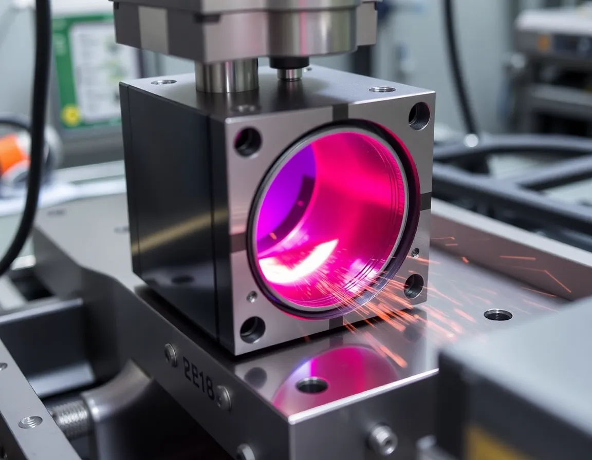
광학 하우징 가공은 광학 시스템 전용의 인클로저, 마운트, 배럴, 브래킷 및 복잡한 섀시를 설계하고 제조하는 과정을 말합니다. 이러한 부품은 뛰어난 수준의 치수 정확도, 열적 안정성, 그리고 종종 복잡한 내부 형상을 달성해야 합니다. 일반 가공과 달리 공차는 종종 마이크론 또는 심지어 서브마이크론 단위로 측정되며, 표면 조도는 미광 산란(다음으로 알려진 현상)을 방지하기 위해 매우 매끄러워야 합니다. 미광). 하우징은 광학 시스템의 골격으로, 요소 간의 정확한 공간 관계를 규정하고 다양한 환경 조건에서도 그 관계가 일정하게 유지되도록 보장합니다.
핵심 구성 요소 및 그 기능
Typical machined parts in an optical assembly include:
- Lens Barrels and Cells: Cylindrical holders that constrain lenses along their optical axis and centrate them radially. They often feature precise threads, shoulders, and retaining rings.
- Mirror Mounts: Kinematic or semi-kinematic mounts that hold mirrors with minimal distortion, allowing for precise tip/tilt adjustment in some applications.
- Optical Benches and Breadboards: Large, stable platforms with precisely located and tapped hole grids for building complex optical trains in laboratories or industrial settings.
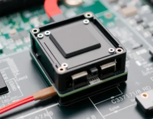
- Sensor Housings: Enclosures that position image sensors (like CCD or CMOS chips) at the exact focal plane of a lens system, often with integrated thermal management.
- Complex Chassis: Multi-faceted housings for devices like binoculars, microscopes, or satellite imaging systems that integrate multiple optical channels and electronic components.
The Machining Process: From Blueprint to Reality
The journey to a perfect optical housing is a multi-stage process demanding close collaboration between optical engineers, mechanical designers, and master machinists.
설계 및 재료 선택
The process begins with a deep understanding of the optical system's requirements. Designers must account for factors like thermal expansion coefficients, stiffness-to-weight ratio, long-term stability (minimizing creep), and sometimes, magnetic permeability. Common materials include:
- Aluminum Alloys (e.g., 6061-T6, 7075): Widely used for their excellent machinability, good strength-to-weight ratio, and moderate cost. Often anodized for wear and corrosion resistance.
- Stainless Steels (e.g., 304, 416): Chosen for high stiffness, superior durability, and low thermal expansion in certain grades. Harder to machine but essential for high-stress or ultra-stable applications.
- Invar (Fe-Ni alloy): Famous for its exceptionally low coefficient of thermal expansion, making it the material of choice for space-based optics and metrology systems where thermal stability is paramount.
- Titanium: Offers an outstanding strength-to-weight ratio and good corrosion resistance, used in aerospace and demanding portable systems.
- Copper and Aluminum-Bronze: Sometimes used for their high thermal conductivity in housings requiring active heat dissipation.
정밀 가공 기술
Once designed, the housing is brought to life using advanced machining technologies:
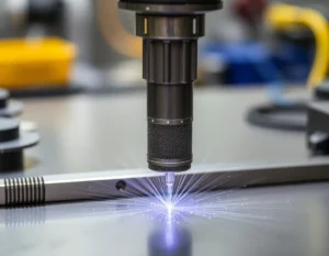
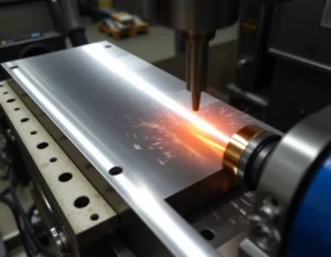
- CNC Milling and Turning: Computer Numerical Control (CNC) machining is the backbone of optical housing production. Multi-axis CNC mills (4-axis, 5-axis) can create complex geometries, internal cavities, and precise mounting features from solid blocks of material with micron-level repeatability.
- Ultra-Precision Diamond Turning: For applications requiring optical-quality surfaces on the housing itself (e.g., reflective inner surfaces, reference flats), single-point diamond turning (SPDT) is employed. This process uses a diamond-tipped tool on a lathe of extreme precision to achieve nanometer-level surface finishes and form accuracy.
- Precision Boring and Honing: For creating perfectly cylindrical, round, and straight bores for lens seats, these processes ensure optimal lens centration and alignment.
- Thread Whirling and Precision Threading: Producing high-accuracy, fine-pitch threads for lens focusing mechanisms or component attachment without inducing runout or misalignment.
Post-Machining: Finishing and Verification
Machining is only part of the story. Critical finishing steps include:
- 응력 제거: Thermal or vibrational stress relieving is often performed to remove internal stresses induced during machining, which could cause the part to warp over time.
- Surface Treatments: Anodizing (for aluminum), passivation (for stainless steel), or specialized blackening processes are applied to enhance durability, prevent corrosion, and reduce surface reflectivity to mitigate stray light.
- Metrology and Inspection: Every critical dimension is verified using high-precision tools like coordinate measuring machines (CMM), laser interferometers, optical comparators, and profilometers. This step is non-negotiable for quality assurance.
Benefits and Applications of Precision-Machined Housings
The investment in high-quality optical housing machining pays dividends across a vast spectrum of technologies.
Key Benefits
- Preserved Optical Performance: Maintains wavefront error, modulation transfer function (MTF), and designed spot size by ensuring perfect alignment.
- Environmental Robustness: Protects delicate optics from shock, vibration, humidity, and temperature fluctuations, ensuring reliability in the field.
- Long-Term Stability: Prevents "drift" in optical alignment over time and through thermal cycles, which is critical for scientific instruments and permanent installations.
- System Integration: Provides a reliable mechanical interface for integrating optics with electronics, actuators, and other subsystems.
Critical Applications
- 항공우주 및 방위: Satellite imaging systems, missile guidance seekers, UAV cameras, and laser targeting systems. Housings must survive launch vibrations and extreme thermal vacuums.
- Life Sciences and Medical: High-resolution microscopes, DNA sequencers, endoscopes, and diagnostic imaging systems (OCT, confocal microscopy). Precision here directly impacts diagnostic capability.
- Semiconductor Manufacturing: Photolithography stepper and scanner lenses, wafer inspection tools. These represent the pinnacle of precision, with housings contributing to nanometer-scale patterning accuracy.
- Telecommunications: Fiber optic alignment ferrules, laser diode packages, and transceiver modules where micron-scale alignment is crucial for signal integrity.
- 소비자 가전: Smartphone camera modules, LiDAR sensors for autonomous vehicles, and VR/AR headsets. Here, precision machining enables miniaturization and mass production of robust optical systems.
Best Practices in Optical Housing Machining
Success in this field hinges on adhering to a set of rigorous best practices.
- Design for Manufacturability (DFM): Involve machinists early in the design phase. Simplify geometries where possible, specify realistic tolerances, and consider tool access for internal features.
- Thermal Management by Design: Integrate thermal considerations from the start. Use symmetric designs to promote uniform expansion/contraction and incorporate mounting strategies that minimize thermal stress on optics.
- Master the Art of Kinematics: Employ kinematic or semi-kinematic mounting principles (using balls, grooves, and planes) to constrain components without over-constraint, which induces stress and distortion.
- Control Stray Light from the Ground Up: Design baffles, light traps, and knife-edges into the housing geometry. Specify low-reflectivity surface finishes (e.g., black anodize, specialized paints) on internal non-optical surfaces.
- Document and Control Processes: Maintain meticulous records of machining parameters, inspection results, and material certifications. This traceability is essential for high-reliability applications and troubleshooting.
- Partner with Specialists: Optical housing machining is a niche expertise. Partnering with machine shops that have proven experience in optics, equipped with the right metrology and a culture of precision, is often the most critical decision of all.
Conclusion: The Foundation of Optical Fidelity
In the relentless pursuit of optical perfection—sharper images, more accurate measurements, more powerful lasers—the significance of the mechanical foundation cannot be overstated. Precision optics are only as good as their mounts. Optical housing machining is the critical bridge between optical design theory and real-world performance. It demands a unique synergy of advanced engineering, state-of-the-art manufacturing technology, and meticulous craftsmanship. By machining the perfect housing, manufacturers do not merely create a container; they build the stable, predictable, and reliable environment in which light can behave exactly as intended, enabling the technologies that define our modern world.